Translate

Tuesday 8 March 2022

Full range analog input for ESP32 ADC


by Giovanni Carrera, 3/03/2022

ESP32 has two 12-bit SAR (Successive Approximation Register) ADCs which are able to convert up to 18 analog inputs. The maximum value to convert is equal to the reference value Vref, for the ESP32 it is about 1 V, but it can vary between 950 and 1100 mV. It is possible to use voltages higher than Vref by attenuating the input. The ESP32 has four possible attenuation options:

Attenuation

input voltage range

ADC_ATTEN_DB_0

100 mV ~ 950 mV

ADC_ATTEN_DB_2_5

100 mV ~ 1250 mV

ADC_ATTEN_DB_6

150 mV ~ 1750 mV

ADC_ATTEN_DB_11

150 mV ~ 2450 mV

In my case, the default attenuation is 0 dB, with an input range of about 68 to 995 mV. For better accuracy it is recommended not to use attenuation, ie 0 dB, and to employ the pins of ADC1, I used GPIO34.

Figure 1 shows a fairly serious problem on low input levels: below 68 mV the converter output gives zero, creating a dead zone and strong non-linearity.
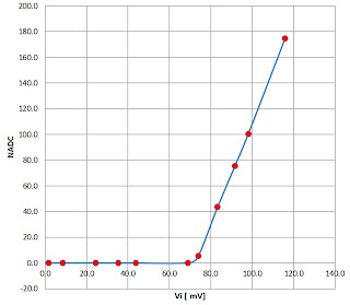
figure 1

So I tried to think of a circuit able to accept an input down to zero volts and to output a signal that can be converted without the drawbacks described above. If, for example, we want to have the following conditions:

Vin = 0 mV → Vout = 100 mV

Vin = 3000 mV → Vout = 1000 mV

The summer circuit, shown in figure 2, realizes these conditions very well.
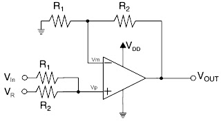
Figure 2


Remembering that for an ideal op amp the inputs are at the same potential, so Vm = Vp , its output voltage is:

Vout = Vp(1+R2/R1)   (1)

Where Vp is the voltage on the non-inverting input of the operational amplifier:

Vp = Vin –(Vin -VR)*R1/(R2+R1)       (2)


In the case of VIN = 0,  we have:

Vp = VR*R1/(R2+R1)

Setting VR = 100 mV, R1 = 300 k and R2 = 100 kΩ, we obtain:

Vout = Vp*4/3

Vp = VR*3/4 = 75 mV

Therefore the output voltage is:

Vout = VR*3/4*4/3 = VR = 100 mV

In the case of VIN = 3000 mV,  from the expression 2 we have:

 Vp = (VIN - VR) *R2/(R2+R1) + VR

And, substituting, we have:

Vp = 3000 –(2900)*3/4= 825 mV

So the output voltage is:

Vout = Vp*4/3 =1100

Setting R1 = 330 kand R2 = 100 kΩ, the conditions imposed are almost perfectly met:

Vin = 0 mV → Vout = 100 mV

Vin = 3000 mV → Vout = 1009 mV

Figure 3 shows the wiring diagram of my prototype. The operational amplifier U1A serves as a voltage follower, U1B as an adder, and U2 provides a stable reference voltage. In my prototype I used the values indicated in the diagram, but I suggest to use the value of 330 k for R2 and R3.

Rail-to-rail operational amplifiers, such as the one indicated, are particularly suitable for this application.
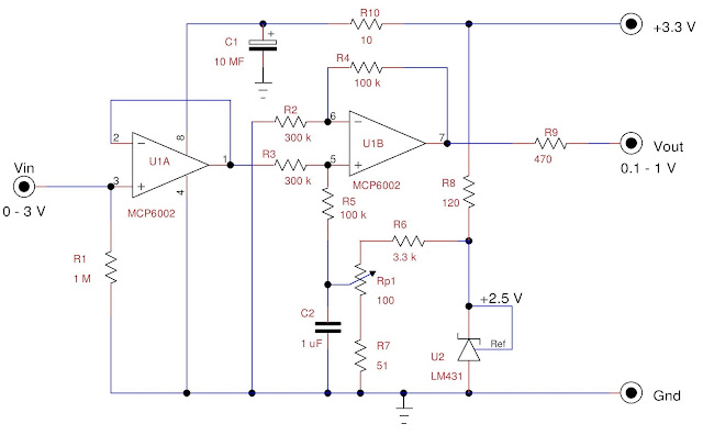
Figure 3


Now you need to perform a calibration. First you have to write a program that reads the values of an analog pin, in my case IO34, and prints them. You can use the Arduino IDE or MicroPython, as in my case.

Put a jumper between the input and ground for Vin = 0, then slowly turn the trimmer Rp1 until you begin to see numbers other than zero.

Figure 4

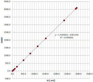
We then connect the Vin input to a low-noise, stable voltage generator, checking the voltage with an accurate digital voltmeter. I take the various measurements and put them on an Excel-like spreadsheet to do a linear regression like the one in figure 4. As can be seen, the results were excellent, with an R2 very close to one. To have the millivolts output, you need to invert the axes of the regression and insert the following expression:

mV = NADC*0.713780799+3.473077

Obviously these values are valid in my case.


Components list

component

description

component

description

R1

1 MW ± 1% metal film

R10

10 W ± 5%

R2, R3

330 kW ± 1% metal film

Rp1

100 Ω multi-turn trimmer

R4, R5

100 kW ± 1% metal film

C1

10 µF,35V Aluminum electrolytic

R6

3.3 kW ± 1% metal film

C2

1 µF,25V ceramic AVX

R7

51 W ± 1% metal film

U1

MCP6002, dual rail-to-rail op amp

R8

120 W ± 5%

U2

TL431, shunt voltage reference

R9

470 W ± 5%


Program

This program, written in MicroPython, acquires 100 samples at 500 Hz, makes the statistics and prints them. I took the average value while also observing the standard deviation of the measurements which must be minimal.

# Program TestADSer.py to test display and ADC

# Giovanni Carrera, 03/03/2022


from machine import Pin,ADC

from time import sleep,sleep_ms

import math


ch1 = ADC(Pin(34))  #   initializes the analog input

ndata = 100

arr = [0 for i in range(ndata)]

while True:

    vmean = 0

    vqmean = 0

    vmax = 0

    vmin = 5000

    for x in range(0,ndata):

        arr[x] = int(ch1.read())

        if arr[x] > vmax :

            vmax = arr[x]

        if arr[x] < vmin :

            vmin = arr[x]

        vmean += arr[x]

        vqmean += arr[x]**2

        sleep_ms(2)

    vmean /= ndata # mean value

    vqmean /= ndata # mean of quadratic values

    k = vqmean - vmean**2

    if k >= 0 :

        StDev = math.sqrt(k)

    else :

        StDev = 0


    print('Analog ch = IO34')

    print('Max =' + str(vmax))

    print('Min=' + str(vmin))

    print('Mean=' + str('%.1f' %vmean))

    print('Sdev=' + str('%.1f' %StDev))

    print()

    sleep(1)


Reference

1.       “AN682 Using Single Supply Operational Amplifiers in Embedded Systems”, Bonnie Baker, Microchip Technology Inc. , 2000

2.       “Analog to Digital Converter (ADC)”, https://docs.espressif.com/projects/esp-idf/en/latest/esp32/api-reference/peripherals/adc.html#adc-calibration

“ESP32 Technical Reference Manual, Version 3.0”, Espressif Systems                                


Sunday 22 August 2021

How to use the SD card of the STM32F407VET6 board with Arduino IDE


This interesting and economical board mounts an ARM Cortex M4 MCU type STM32F407VET6 produced by ST Microelectronics and is also called “black board” or “black pill” due to the dark color of the pcb. There are several versions, the one I used is shown in figure 1.

Figure 1 -The Black Board

The MCU has 100 pins (LQFP100 package), so it is suitable for those applications where a lot of I/O and also a remarkable speed of execution are required. Its main features are: 168MHz clock, 512KB of Flash memory, 128KB of RAM, 82 GPIO (many of which 5 volt tolerant), 16 12-bit analog channels, 2 12-bit DAC channels, a USB OTG port and many other things. Among these, a 32768 Hz crystal RTC and 4kB of RAM rendered non-volatile by the backup stack.

I bought this interesting and inexpensive card not only for the reasons mentioned above but also because it had an micro SD card connector. I had already done several projects with the STM32F103C8T6 board, also called “bluepill”, compiling with Arduino IDE after loading the package and I wanted to experiment on bigger systems too.

The SD card

It is not connected to the SPI bus but to the SDIO bus and the Arduino libraries use the SPI. To be able to use the more performing SDIO interface, you need to change the development environment, but I didn't want to do this.

To overcome this obstacle I connected the SD to an SPI bus with three external wires connected to the pins available on the various connectors. This is easily achieved by connecting the pins with the wires headed with female Dupont connectors the card is equipped with. The original connections do not go into conflict as I initialize them as a pull-up input, therefore, inserting the resistors that were missing.

SPI pin

J2


SD pin

J3

name

PA7

30

«

PD2

24

SPI1 MOSI

PA6

29

«

PC8

37

SPI1 MISO

PA5

28

«

PC12

27

SPI1 SCK

Table 1 – Wiring to do for SPI bus

As you can see in the table, the pins connected to the SD are all on the J3 connector and the pins of the SPI bus are all on the J2 connector. Pin 1 of the connectors is always indicated by a square pad, on the soldered side. Pin PC11, connected to the SD (DAT3 = CS) is fine, just indicate it in the initialization of the SD.

At the top of the program, among other instructions, these should be placed:

#include <SPI.h>
#include <SD.h>
#define SD_MOSI PA7
#define SD_MISO PA6
#define SD_CLK PA5
#define SD_CS PC11
boolean SDok;


The following instructions must be entered in the setup () function:

  pinMode(PD2, INPUT_PULLUP);// SDIO pin
  pinMode(PC8, INPUT_PULLUP);// SDIO pin
  pinMode(PC12, INPUT_PULLUP);// SDIO pin
  SPI.setMOSI(SD_MOSI);
  SPI.setMISO(SD_MISO);
  SPI.setSCLK(SD_CLK);
  if (!SD.begin(SD_CS)) {
    SDok = false;
  } else {
   SDok = true;
  }

The tests gave positive results with the SD.h library and negative with STM32.h.

With this simple trick I could also use the SD card with Arduino IDE.


Monday 6 April 2020

How to sterilize corona virus masks


Introduction
First of all, I want to reiterate that I am not responsible for what I will expose in this article, it is just an idea that came to me reading that ultraviolet rays alter the DNA of viruses and make them harmless. To have a scientific validity it is necessary to know other information such as the intensity of UV radiation and the exposure time necessary to eliminate them. In these times of forced isolation, I thought of reusing the lamp of an old eprom (Erasable Programmable Read-Only Memory) eraser that I had at home. These non-volatile memory chips had a fused quartz window to erase them by exposing them to a special ultraviolet lamp for a few tens of minutes.

The lamp
The recommended exposure time for eproms was 20-30 minutes with a UV lamp with a wavelength of 253.7 nm with an intensity of at least 15W / cm2 and at a distance of approximately 2.5 cm.
The lamp of my eraser, shown in figure 1, may have similar characteristics.
Figure 1
It is a transparent fluorescent tube, having no internal phosphor coating, with a power of 6W. The lamp housing is made of fused quartz or Vycor as the common glass filters UVC rays. The efficiency is around 30-40%, which means that the effective radiated power is at most 2.4W so it is necessary to use an aluminum reflector to put under the lamp, as seen in the prototype photos. Even a thin sheet of aluminum, like the one used in the kitchen, acts very well as a reflector.
As you can see from the photo, the lamp has the writing "GERMICIDAL" G6T5 GL-6. It is not difficult to find them on the market because they are widely used for disinfection of air and water. Philips also produces several lamps with a wavelength of 253.7 nm (UVC) from the TUV TL series. The cost is less than 10 €.
Warning, UVC lamps are very harmful to the eyes and skin, therefore all precautions must be taken, as I did in my project.
The lamp, like all fluorescent tubes, requires a ballast suitable for its power and a starter.
A tanning lamp (UVA) is not good or, in any case, does not have the same effectiveness.
Even the black fluorescent tubes, coated with special phosphors that filter the visible light (> 400 nm), emit UVA radiation.

Germicidal lamps made with UVC led arrays are also on the market, but these are of higher wavelength (265-290 nm). From what I have seen in the datasheets, these LEDs have not high powers and low efficiency (10%), therefore different ones are needed and they are also quite expensive.

My realization
I made my system with what I had at home. I disassembled the lamp, ballast, starter and timer from the old eraser and mounted them in a suitably sized aluminum cabinet, as seen in the images in figure 2.


Figure 2

On the bottom right side I mounted a micro-switch to turn off the lamp when the cover is open, as seen in figure 3. The timer used is mechanical.
Figure 3

Of course you could make this system in better ways, perhaps by inserting a support for the mask, but I made it with what I had at home.
The green light that can be seen at the top acts as a simple slide, lights up with the light of the lamp and indicates that it is working.
The scheme is shown in figure 4.
Figure 4

Parts list
  • 6W UVC lamp (254 nm) Philips TUV TL or Osram HNS 6 W G5 or compatible.
        2 lamp holders with G5 socket.
        Starter complete with 6-9W ballast or electronic ballast.
        Micro-switch.
        0.5 A fuse and fuse holder.
        Double switch, power cord with earth.
        1-5 minutes electronic or mechanical timer.
        25x15x10 cm aluminum case.
        21x12 cm aluminum reflector, 4 + 4 + 4 cm folded (trapezoidal section).


References
1.       “Ultraviolet”, https://en.wikipedia.org/wiki/Ultraviolet
2.       “Philips TUV TL Mini”,

3.       “HNS 6 W G5, PURITEC HNS UV-C”, OSRAM GmbH, April 17, 2020

Wednesday 1 April 2020

A DIP switch for Arduino

How to read a quad dip switch with only one analog pin with Arduino

The DIP switch is a set of small switches in a Dual In-line Package. It finds numerous applications, such as address configurator, select a type of operation, enter a remote control code.

Normally the dip switches require as many digital input pins as there are dip switches used and also with pull-up resistors enabled. In the proposed circuit I use only one analog input for four dip switches.

This article is also particularly useful for applications with ESP8266 which has few I/O pins but has an analog input with a full-scale of 1V.

After developing a project to read a 4x3 keypad with three analog inputs [1], I was thinking of applying this methodology to dip switches too but things are not at all similar. The buttons close only one at a time and are monostable while the dip are bistable and also can close all together.
After several attempts, simulated at computer, I arrived at the synthesis of the circuit shown in figure 1.
Figure 1
In theory, the values of the R1-R4 resistors should be 1, 2, 4, 8 kΩ, but even with the standard values I used, good results are obtained. If we measure the resistance between Vo and Gnd, we have a value that is proportional to the binary number set, but the Vo voltage will be equal to:
Vo = Vcc*R14/(R5+R14)
Where with R14 I indicated the sum of the resistors R1 to R4 not short-circuited by the dip switches. As can be seen, now the law is not linear, but it suffices to put R5 large enough to minimize the current variation. This will reduce the output voltage, but by setting the Arduino reference voltage as "INTERNAL" we get a full-scale Arduino UNO ADC converter equal to about 1.1V.
Indicating with "ON" the closed switches and with "OFF" the open ones and setting Vcc = 5V the following table is obtained.
D4
D3
D2
D1
N
R14
I [mA]
Vo [mV]
DV [mV]
NADC
DN
NADC_L
NADC_H
ON
ON
ON
ON
0
0
0.073
0.00
0
0
0
0
30
ON
ON
ON
OFF
1
1000
0.072
72.36
72.36
67
67
47
87
ON
ON
OFF
ON
2
2000
0.071
142.65
70.29
133
66
113
153
ON
ON
OFF
OFF
3
3000
0.070
210.97
68.32
196
63
176
216
ON
OFF
ON
ON
4
3920
0.069
272.15
61.18
253
57
233
273
ON
OFF
ON
OFF
5
4920
0.068
336.89
64.75
313
60
293
333
ON
OFF
OFF
ON
6
5920
0.068
399.89
63.00
372
59
352
392
ON
OFF
OFF
OFF
7
6920
0.067
461.21
61.32
429
57
409
449
OFF
ON
ON
ON
8
8200
0.066
537.35
76.14
500
71
480
520
OFF
ON
ON
OFF
9
9200
0.065
595.08
57.73
553
53
533
573
OFF
ON
OFF
ON
10
10200
0.064
651.34
56.26
606
53
586
626
OFF
ON
OFF
OFF
11
11200
0.063
706.18
54.84
657
51
637
677
OFF
OFF
ON
ON
12
12120
0.062
755.42
49.24
703
46
683
723
OFF
OFF
ON
OFF
13
13120
0.062
807.68
52.26
751
48
731
771
OFF
OFF
OFF
ON
14
14120
0.061
858.67
50.99
799
48
779
819
OFF
OFF
OFF
OFF
15
15120
0.060
908.44
49.76
845
46
825
865
Where NADC is the output number of the 10-bit ADC converter. With four dip we represent 2^4 = 16 different states that must be identified precisely. The program must discriminate each state with two thresholds NADC_L (lower) and NADC_H (upper). The number of 10 bits, at the converter output, must be between these two limits which I determined with ± 20 units with respect to the NADC value. The diagram in figure 2 clearly shows the intervals and the output voltage Vo as a function of the number set on the four dip.
Figure 2
As can be seen, the trend is fairly linear and the intervals DN range from a minimum of 46 to a maximum of 71, so the thresholds of ± 20 do not overlap.
As shown in the table, by powering the circuit with Vcc = 5V, the maximum output voltage is 908.44 mV, lower than the maximum voltage (1100 mV) accepted by the converter.
If you need an 8-pin dip switch, just duplicate the circuit and use a second analog input. Figure 3 shows a connection diagram of the individual components.
Figure 3

The circuit is realized with few soldered joints and it is also easy to draw the printed circuit. Figure 4 shows the appearance of my prototype seen from the component side and from the soldered side. I used a small perforated circuit board of about 40x30 mm.
I have optimized the circuit for Arduino / Genuino Uno and the program is fine for MCU type ATmega328 / 168. But it can also be used, with minor modifications, with other MCUs, such as SAMD21G18 mounted on Arduino Zero and Arduino MKR1000 boards and also ESP8266 and 32.
Figure 4
I used a 3-pin strip connector for wiring with Arduino. The resistors must have a low tolerance, I used those with 1/4W metal film with a tolerance of ± 1%, very common and easy to find. Figure 5 shows the wiring between the DIP card and Arduino Uno.
Figure 5

List of components
component
description
component
description
R1
1 kW ± 1% metal film
R5
68.1 kW ± 1% metal film
R2
2 kW ± 1% s metal film
-
0.1” perforated circuit board
R3
3.92 kW ± 1% metal film
-
3 pin strip connector
R4
8.2 kW ± 1% metal film
Dip4
DIP switch with 4 positions

The program
The sketch is an example of use of the circuit and provides both the number and the individual dip arranged in the DipSw char array. In this example I use Arduino Uno's pin A0 as an analogue input and in the setup I insert the analogReference (INTERNAL) instruction to set the internal Vref at 1.1V, more stable and less noisy than the default at 5V.
In the loop () function I set the discrimination to thresholds and in the readDIP function (byte mybyte) I create the array of characters ordered as the dip switches. This last function is useful to use every single switch.

/* program DIP4to1.ino
 *  only one analog input for 4 dip switches
 *  Giovanni Carrera - 20/08/2019
 */
int DipPin = A0;// DIP4 analog input
// limits of DIP4 output values:
const int NADC_L[16] = {0,47,113,176,233,293,352,409,480,533,586,637,683,731,779,825};
const int NADC_H[16] = {30,87,153,216,273,333,392,449,520,573,626,677,723,771,819,865};
char DipSw[5];

void setup(){
 analogReference(INTERNAL); // internal ADC reference input = 1100V
 Serial.begin(115200); // used with serial monitor
}

void loop() {
  int val = analogRead(DipPin);// read analog keyboard
  for (int i=0; i < 16; i++){
     if (val >= NADC_L[i] && val <= NADC_H[i]){// has found the right value
        Serial.print(val);
        Serial.print(" , N = ");
        Serial.print(i);
        Serial.print(" , Dip = ");
        readDIP(i);
        Serial.println(DipSw);
        break;
     }
  }
  delay(500); 
}

void readDIP(byte mybyte){
 byte mask = 0x01;
 for(int i=3; i >= 0; --i){
   if(mask & mybyte)
       DipSw[i]= '1';
   else
       DipSw[i]= '0';
   mask <<= 1;
 }
}

References
1.      “Very few wires for a numeric keypad for Arduino”, Giovanni Carrera, 10/11/18, http://ardupiclab.blogspot.it
2.       “Only Three Pins for a 4x3 Keypad”, Giovanni Carrera,  November 19, 2018, https://www.hackster.io